Dit is een printplaat van een schip. Een onderdeel was zwaar verbrand en de printplaat was door en door verbrand. Dit moest zo origineel mogelijk hersteld worden, het mocht niet met wat draadjes. Zowiezo moet er dan meer gebeuren want het zwarte spul geleidt stroom.
It had burned through the whole thickness of the PCB. It was possible to just add some wires instead of the burned traces but that was not allowed. Besides that, burned PCB is conductive.
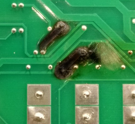
Ik was vergeten een foto te maken van de bovenkant. Deze was het ergst verbrand.
I forgot to take a picture from the top that was the most burned and I already cleaned a part of the bottom. But it turned out it was burned through and through.
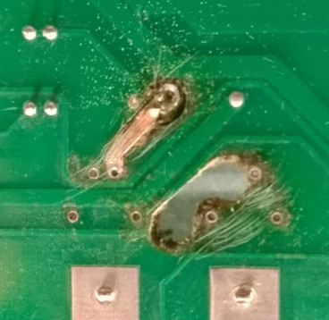
Ik heb al het verbrande materiaal weg gefreesd. Dat betekende ook dat een paar traces en vias opgeofferd moesten worden. Niet echt een probleem maar als het even kan liever niet.
I milled out all the burned material. A few vias and traces had to go. Not a big problem but if possible (no damage) I spare them.
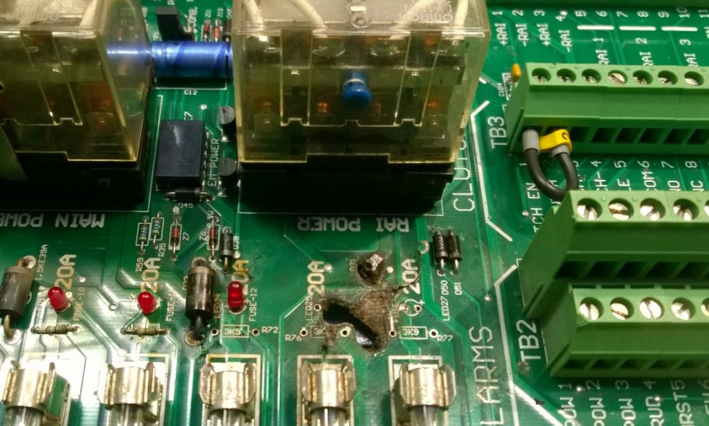
De boel was through hole en dat maakt het wat lastiger. SMD is makkelijker omdat je geen pootje hebt wat het pcb intern roostert.
To show the scale. It was all through hole but that makes it not always more easy. SMD can be more easy because there is no hot component pin burning in the PCB itself.
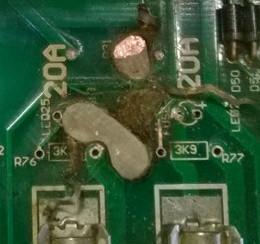
Making a replacement PCB insert is not difficult but takes some time. Getting it at the right thickness was harder. If there were inner layers I would have made several layers but this was only two sided so I could use one layer. The epoxy for the new traces is the most critical because I need to solder to them. Making and mounting the new vias and new traces is the most difficult part. Because this had to be better as it was, I made much thicker traces. For that I had to mill some PCB material to embed the new trace partly into the PCB so it looks like it was.
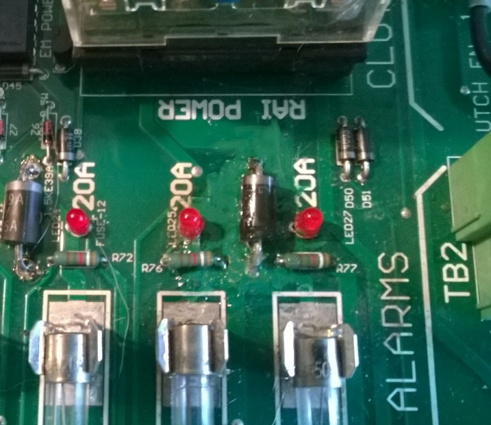
Dit is het resultaat na reparatie en “verven”. Er zit ook wat siliconen conformal coating over heen als bescherming. Het oogt daardoor wat rommelig. Het is niet zoveel werk (ik doe dit regelmatig) maar het kost nogal wat tijd. De epoxies die ik gebruik zijn hittebestendig en het duurt een paar dagen voor ze hard genoeg zijn om te solderen. Daarnaast moet het meestal in lagen. Dit was tweezijdige print maar ik heb dit ook bij 4 laags printen gedaan waarbij ik ook inner-layers moest herbouwen. Nieuwe vias maakt het ook wat lastiger, vooral bij dit soort dikke pcbs.
This is the result after applying some new green PCB paint. And to protect everything I added some silicon con formal coating. It makes it a bit messy looking but just to be sure. On the picture the coating looks much more visible as it was. All in all this is not that much work but it takes time because things like the epoxy need a few days to hard.